- 您现在的位置:买卖IC网 > Sheet目录1233 > NCP1031POEEVB (ON Semiconductor)BOARD EVAL NCP1031 POE DC CONV
�� �
�
�NCP1030,� NCP1031�
�be� limited� by� the� EA� sink� current,� typically� 110� m� A.�
�Optimum� transient� response� is� obtained� if� the� compensation�
�is� discharging,� guaranteeing� a� maximum� duty� cycle� of� 75� %�
�as� shown� in� Figure� 35.�
�components� allow� COMP� to� swing� across� its� operating�
�range� in� 1� cycle.�
�Line� Under� and� Overvoltage� Detector�
�C� T� Ramp�
�COMP�
�Enabled�
�C� T� Charge�
�Signal�
�The� NCP103x� incorporates� individual� line� undervoltage�
�(UV)� and� overvoltage� (OV)� shutdown� circuits.� The� UV� and�
�OV� thresholds� are� 2.5� V.� A� fault� is� present� if� the� UV� is� below�
�2.5� V� or� if� the� OV� voltage� is� above� 2.5� V.� The� UV/OV�
�detectors� incorporate� 175� mV� hysteresis� to� prevent� noise�
�from� triggering� the� shutdown� circuits.�
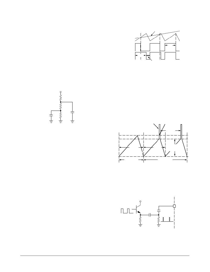
�The� UV/OV� circuits� can� be� biased� using� an� external�
�resistor� divider� from� the� input� line� as� shown� in� Figure� 34.�
�The� UV/OV� pins� should� be� bypassed� using� a� capacitor� to�
�prevent� triggering� the� UV� or� OV� circuits� during� normal�
�switching� operation.�
�V� in�
�R� 1�
�+�
�R� 2�
�+� V� UV�
�V� OV� R� 3�
�--� --�
�Figure� 34.� UV/OV� Resistor� Divider�
�from� the� Input� Line�
�The� resistor� divider� must� be� sized� to� enable� the� controller�
�Power� Switch� Max�
�Duty� Cycle�
�75%�
�25� %�
�Figure� 35.� Maximum� Duty� Cycle� vs� COMP�
�Figure� 18� shows� the� relationship� between� the� operating�
�frequency� and� C� T� .� If� an� UV� fault� is� present,� both� I� CT(C)� and�
�I� CT(D)� are� reduced� by� a� factor� of� 7,� thus� reducing� the�
�operating� frequency� by� the� same� factor.�
�The� oscillator� can� be� synchronized� to� a� higher� frequency�
�by� capacitively� coupling� a� synchronization� pulse� into� the� C� T�
�pin.� In� sync� mode,� the� voltage� on� the� C� T� pin� needs� to� be�
�driven� above� 3.5� V� to� trigger� the� internal� comparator� and�
�complete� the� C� T� charging� period.� However,� pulsing� the� C� T�
�pin� before� it� reaches� 3.5� V� will� reduce� the� p--p� amplitude� of�
�the� C� T� Ramp� as� shown� in� Figure� 36.�
�3.0� V/3.5� V�
�Sync� Pulse� Comparator�
�Reset�
�T2� (f2)�
�3.5� V�
�once� V� in� is� within� the� required� operating� range.� While� a� UV�
�or� OV� fault� is� present,� switching� is� not� allowed� and� the�
�COMP� pin� is� effectively� grounded.�
�C� T�
�Ramp�
�T1� (f1)�
�T2� (f2)�
�C� T� Voltage�
�Range� in� Sync�
�Either� of� these� comparators� can� be� used� for� a� different�
�function� if� UV� or� OV� functions� are� not� needed.� For� example,�
�the� UV/OV� detectors� can� be� used� to� implement� an� enable� or�
�3.0� V�
�Free� Running�
�Mode�
�Sync� Mode�
�disable� function.� If� positive� logic� is� used,� the� enable� signal�
�is� applied� to� the� UV� pin� while� the� OV� pin� is� grounded.� If�
�negative� logic� is� used,� the� disable� signal� is� applied� to� the� OV�
�pin� while� biasing� the� UV� pin� from� V� CC� using� a� resistor�
�divider.�
�Oscillator�
�Figure� 36.� External� Frequency� Synchronization�
�Waveforms�
�The� oscillator� frequency� should� be� set� no� more� that� 25%�
�below� the� target� sync� frequency� to� maintain� an� adequate�
�voltage� range� and� provide� good� noise� immunity.� A� possible�
�circuit� to� synchronize� the� oscillator� is� shown� in� Figure� 37.�
�The� oscillator� is� optimized� for� operation� up� to� 1� MHz� and�
�its� frequency� is� set� by� the� external� timing� capacitor� (C� T� )�
�connected� to� the� C� T� pin.� The� oscillator� has� two� modes� of�
�operation,� free� running� and� synchronized� (sync).� While� in�
�free� running� mode,� an� internal� current� source� sequentially�
�charges� and� discharges� C� T� generating� a� voltage� ramp�
�between� 3.0� V� and� 3.5� V.� Under� normal� operating�
�conditions,� the� charge� (I� CT(C)� )� and� discharge� (I� CT(D)� )�
�currents� are� typically� 215� m� A� and� 645� m� A,� respectively.� The�
�5V�
�R1�
�C1�
�C� T�
�R2�
�C� T�
�2�
�charge:discharge� current� ratio� of� 1:3� discharges� C� T� in� 25� %�
�of� the� total� period.� The� Power� Switch� is� disabled� while� C� T�
�Figure� 37.� External� Frequency� Synchronization�
�Circuit.�
�http://onsemi.com�
�14�
�发布紧急采购,3分钟左右您将得到回复。
相关PDF资料
NCP1605LCDTVGEVB
BOARD EVAL NCP1605/1396
NCP1608BOOSTGEVB
BOARD EVAL NCP1608 100W BOOST
NCP1631PFCGEVB
BOARD DEMO NCP1631 INTERLEAV PFC
NCP1650EVB
BOARD EVAL NCP1650 PFC CTLR
NCP1652L48VGEVB
BOARD EVAL 100W 48V NCP1652 PFC
NCP1653EVB
BOARD EVAL FOR NCP1653
NCP2993FCT2GEVB
BOARD EVAL NCP2993 AUDIO PWR AMP
NCP345SNT1G
IC DETECTOR OVER VOLTAGE 5TSOP
相关代理商/技术参数
NCP1034
制造商:ONSEMI 制造商全称:ON Semiconductor 功能描述:100V Synchronous PWM Buck Controller
NCP1034BCK5VGEVB
功能描述:电源管理IC开发工具 48/5V 5A SYNC BCK
RoHS:否 制造商:Maxim Integrated 产品:Evaluation Kits 类型:Battery Management 工具用于评估:MAX17710GB 输入电压: 输出电压:1.8 V
NCP1034DR2G
功能描述:DC/DC 开关控制器 HV PWM BUCK CONTROLR RoHS:否 制造商:Texas Instruments 输入电压:6 V to 100 V 开关频率: 输出电压:1.215 V to 80 V 输出电流:3.5 A 输出端数量:1 最大工作温度:+ 125 C 安装风格: 封装 / 箱体:CPAK
NCP1050
制造商:ONSEMI 制造商全称:ON Semiconductor 功能描述:Monolithic High Voltage Gated Oscillator Power Switching Regulator
NCP1050/D
制造商:ONSEMI 制造商全称:ON Semiconductor 功能描述:Monolithic High Voltage Gated Oscillator Power Switching Regulator
NCP1050_06
制造商:ONSEMI 制造商全称:ON Semiconductor 功能描述:Monolithic High Voltage Gated Oscillator Power Switching Regulator
NCP1050P100
功能描述:交流/直流开关转换器 700V 100mA Switching RoHS:否 制造商:STMicroelectronics 输出电压:800 V 输入/电源电压(最大值):23.5 V 输入/电源电压(最小值):11.5 V 开关频率:115 kHz 电源电流:1.6 mA 工作温度范围:- 40 C to + 150 C 安装风格:SMD/SMT 封装 / 箱体:SSO-10 封装:Reel
NCP1050P100G
功能描述:交流/直流开关转换器 700V 100mA Switching No Auxillary Winding RoHS:否 制造商:STMicroelectronics 输出电压:800 V 输入/电源电压(最大值):23.5 V 输入/电源电压(最小值):11.5 V 开关频率:115 kHz 电源电流:1.6 mA 工作温度范围:- 40 C to + 150 C 安装风格:SMD/SMT 封装 / 箱体:SSO-10 封装:Reel